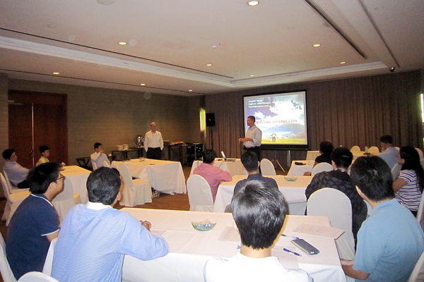
At an industry event last Friday (Oct 14th 2011), we had the chance to present a talk on, "What Can FPGA Designers Do With Personal Data Centers?" and demonstrate our new cloud-based approach to achieving timing closure for an FPGA design.

Opening
Mike Holt, Vice-President of the Singapore Semiconductor Industry Association, opened the event with a look at this "cloud thingie" and how rising complexity of chip designs cause hardware designers problems in design and verification processes. Consequences include expensive product delays and bigger development bills. The cloud approach is increasingly seen as a good solution.
Background on cloud computing
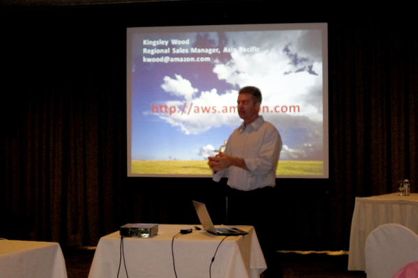
Kingsley Wood from Amazon Web Services (AWS) continued along this vein with an introduction to cloud computing, highlighting AWS features that might be of interest to a solutions provider like us. Specific to the semiconductor industry where compute-intensive tasks, large file sets and complex workflows abound, and with major EDA vendors already using the AWS infrastructure to provide some services, cloud computing has certainly become significant for chip design.
Members of the audience were curious as to how annual licensing schemes for enterprise software have been changed into SaaS models in other industries, and how AWS and solution providers of cloud computing applications deal with data losses.
IC Design-specific issues
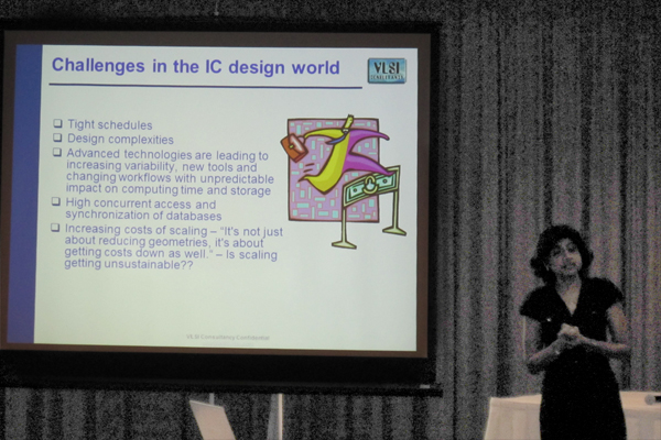
Meenu Sarin from VLSI Consultancy was up next, talking about specific challenges such as portability of design data in multi-vendor flows, standardization of IP and difficulties in scaling design processes. She also explored concerns about the cloud such as security and bandwidth, and raised the question of which organizations are best-suited to manage a cloud resource in the semiconductor industry where there are so many different stakeholders.
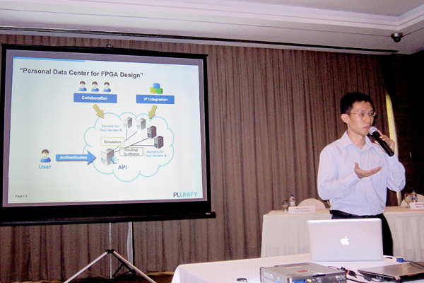
Personal data center for FPGA design
What does a designer think of when s/he sees the term, "data center for FPGA design"?
We proposed the model of a dedicated resource with the requisite components for an FPGA design:
- IP to use in the design
- Tools (and licenses) to crunch the design
- Servers to run the tools
- Collaboration mechanisms e.g. source control, permissive sharing
- Portability of data (standardization) if/when a multi-vendor approach is desired
- Pay-as-you-use
The above framework is by no means groundbreaking, as since the 1960s, our industry has seen mainframes and supercomputers in a centralized processing model evolve into dispersed workstations and distributed grid computing networks, all before cloud computing came into fashion. However, to us, scalability is the most attractive thing about the cloud, the best thing since sliced cloud.
Demo
I then proceeded to show, "live", how an FPGA design that fails timing can be processed in parallel, using a cloud managed by Plunify, to achieve timing closure.
- Linux PC connected to the Internet via a Wifi network
- Altera Quartus II 10.0 SP1
This is meant to mimic a typical designer's setup
- OR1200 32-bit microprocessor
- Altera Stratix III L50 FPGA
- Plunify plugin scripts for Quartus
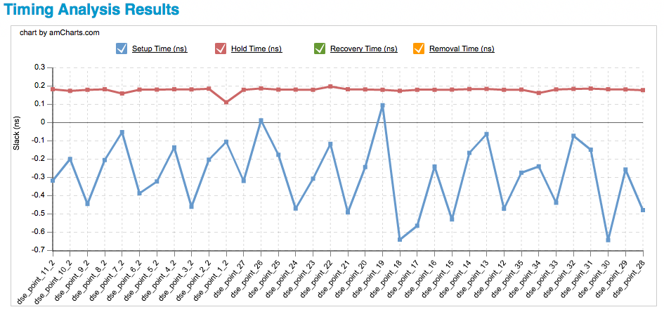
Initially, there's a Timing Violation (Slack) of -0.519 ns
Using a cloud-based approach, our tool calculates a series of parameters that will help the place-and-route tool, and then from the Linux PC, runs all these iterations in parallel.
Out of 35 iterations, each taking about 30 minutes, two iterations met timing.
- Timing closure was achieved at 0.093 ns, 0.011 ns. *phew*!
- Summary: http://www.plunify.com/reports/timingAnalysis.php?or1200_top=1
- Only iterations "dse_point_19" and "dse_point_26" had the passing timing results. (Mouse-over the "i" icons in the table to see which parameters were used in each iteration (revision).
The demo went well, (to my relief - presenter anxiety!), and immediately the audience could see our cloud-based approach got to timing closure in almost 1/20 of the amount of time that would have been spent.
Let us know how useful this feature is - tellus (at) plunify (dot) com
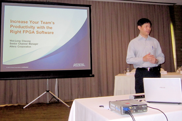
Productivity features in FPGA tools
Wai-Leng Cheong, Sr Channel Manager at Altera proceeded to describe incremental compilation features of the Quartus II software, and how it can be used as a form of collaboration by design teams working at different locations. Among other things, the Quartus software makes use of multiple CPU cores which makes it even more well-suited to a cloud environment.

Panel Discussion
The last formal item for the event was a discussion where we talked about more high-level issues and the implications of cloud computing in the industry for end-users and vendors alike. Topics included:
- Companies are finding different ways to speed up development, for example, improving software algorithms in tools, using hardware emulation platforms standalone or to augment software simulations, streamlining workflows and procedures, etc.
- Cloud computing, though much hyped in general, is one way to improve time-to-market, and its economies of scale makes it especially compelling.
- Lack of a common design methodology, data standards are some of the deeper issues that cause delays in the semiconductor industry.
- Changes to the current annual licensing model must be justifiable in order to persuade tool vendors to switch to a hourly / daily / weekly / monthly / pay-as-you-use model. However the longer that process takes, the riskier it might become for vendors in the long run because the costs of sustaining the annual licensing model are becoming more and more daunting. EDA vendors have been facing slowing growth for a few years now.
- Besides solutions providers, are foundries the natural candidates for the managers of a cloud solution?
Because the economies of scale make so much more sense for both vendors and users alike, we have to work hard to put together scenarios whereby a change from the traditional annual licensing model to an hourly / daily / weekly / monthly model does not erode the bottom-line for companies which have been relying on the former for so long.
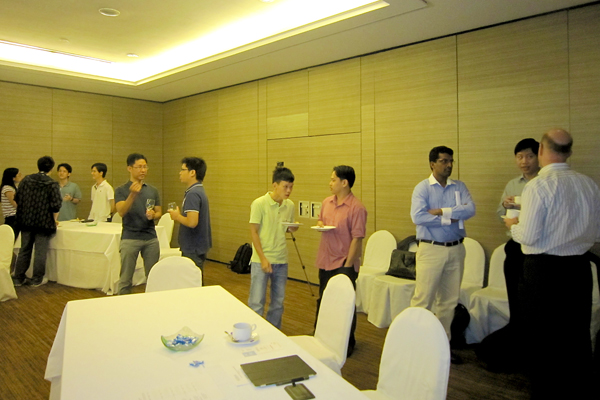
It was a pleasure to be a part of this event organized by the Singapore Semiconductor Industry Association (SSIA) and to meet fellow semiconductor professionals and hardware designers from local schools, research labs and companies.
- harnhua
Thanks for sharing your info. I really appreciate your efforts and I will be waiting for your further write ups thanks once again.
January 25, 2012 at 12:17 pmSEO tools